
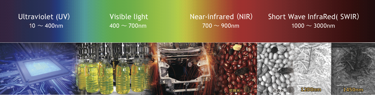
The Place of Ultraviolet in the Electromagnetic Spectrum
The human eye is sensitive to only a tiny sliver of the electromagnetic spectrum – the wavelengths between ~400 (violet) and 700 (red) nanometers, the portion we call light. Some other animals can see beyond these endpoints: bees, for instance, use ultraviolet sensitivity in their eyes to detect pollen, while many animals detect prey at night using infrared radiation – which is essentially body heat. But humans need external devices, such as specially-designed cameras, to sense wavelengths beyond the visible part of the spectrum.
Most people have some familiarity with “night vision” thermal cameras or binoculars which reveal people, wildlife, and other objects by capturing their “heat signatures” in the form of infrared radiation. But ultraviolet radiation – which lies between 10 and 400 nanometers – is much less familiar to most people because there are fewer consumer devices that probe beyond this end of the visible spectrum.
Probing what the eye cannot see
To create images, cameras rely on a fundamental principle of physics called the “Law of Reflection.” Similar to a tennis ball thrown against a wall, electromagnetic radiation – whether visible light or non-visible wavelengths – is reflected off surfaces based on the angle at which it strikes the “wall.”
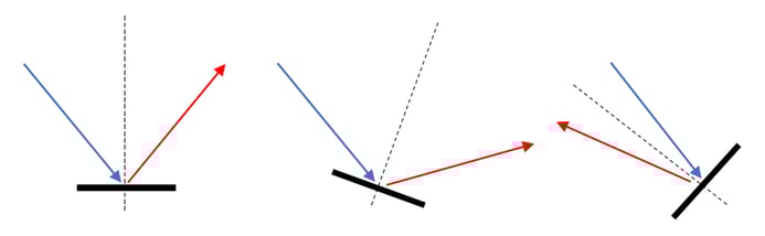 The law of reflection
More importantly, imaging is made possible by the fact that most surfaces are not perfectly smooth when viewed at a microscopic (or nanoscopic) level. These surface irregularities cause a “diffuse reflection” where, although individual light rays still follow the Law of Reflection, the different angles they encounter on the surface cause reflections in many different directions, sending some portion of the light back to a person or camera viewing the scene.
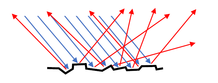 Diffuse reflection
The size of surface features that cause diffuse reflection depends on the wavelength of the light striking the surface. If surface features are less than about one-eighth of the wavelength of the light, the surface is said to be polished and light rays all bounce off the surface in the same direction producing a mirror effect. In this case, the tiny surface irregularities become invisible to the viewer or camera.
Because of its shorter wavelengths, ultraviolet radiation is diffused by smaller surface irregularities that may have no effect on longer wavelengths. This enables UV imaging to detect and inspect extremely small surface features and/or defects that simply cannot be seen under visible light.
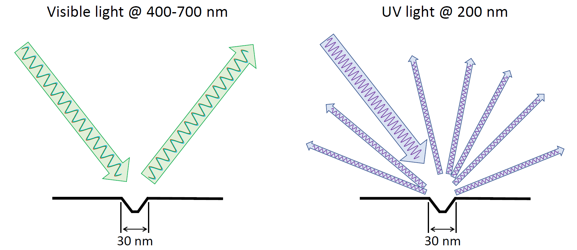
Short wavelengths are diffused by small surface features
A growing number of industrial applications are leveraging the way small surface features reflect UV wavelengths. These include a range of semiconductor inspection tasks like mask inspection, checking for wafer defects, pattern defect identification and classification; surface inspection of plastic and metal surfaces for microscopic defects; and solar panel inspection.
Other uses for UV imaging take advantage of the way certain inks and materials absorb UV radiation or fluoresce in the UV spectrum. Some of these applications include print inspections of pharmaceutical packaging, passports, and banknotes; sorting of waste materials; nondestructive testing of materials for defects and impurities; fluorescence analysis for fraud detection and criminal forensics; medical diagnostics, and many more. UV imaging is also used for corona inspection of high-voltage transmission lines and in various scientific applications including those for astronomy, microscopy, and UV spectroscopy. The images below illustrate some examples of the applications of UV-based imaging.
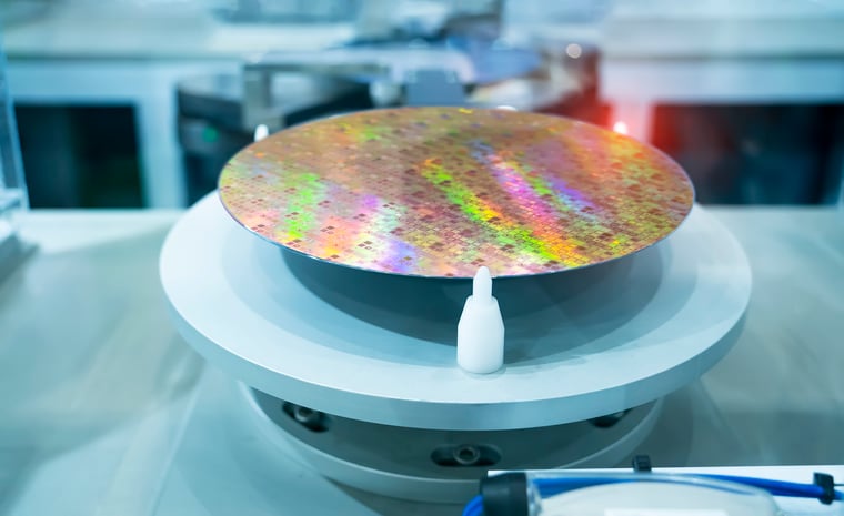 Figure 1: Production of wafer disc
Figure 1 shows the use of UV imaging in the electronics industry, where the lasered codes on the reflective surface of wafer discs must be reliably read to pinpoint and trace each wafer through the production process – otherwise the production chain halts, with serious financial consequences. UV imaging can reliably read these codes, which conventional machine vision systems cannot.
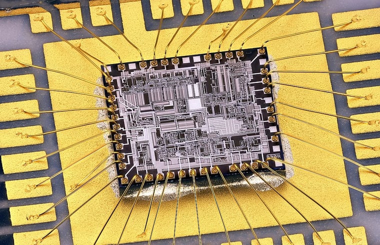 Figure 2: UV imaging used for die/wire bonding. Author:Mister_rf
The image in Figure 2 shows the use of UV imaging for semiconductor alignment. UV imaging is used in semiconductor manufacturing to ensure proper wafer probing, wafer dicing, lead frame inspection, and die/wire bonding.
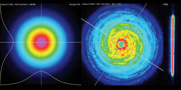 Figure 3: Laser beam profiling. Source: Photonics.com
In Figure 3 above, the precision of a laser beam such as its shape and size affects the energy it delivers at a target. Distortions of the beam arise from contamination in the optical path, errors in assembly, and environmental factors. By inserting a UV camera in the beam path, the relative intensity of each portion of the beam can be mapped – and corrected.
Equipping Vision Systems with UV Industrial Cameras
The high demand for the many types of UV optical inspections described here has greatly increased the scope of applications for ultraviolet (UV) imaging cameras. Vision systems incorporating cameras with UV image sensors can provide special visual information that ordinary cameras cannot. These include systems equipped with both UV-compatible lenses and UV lighting for typical industrial and scientific applications, as well as laser profiling systems where lenses and even the cover glass on the sensor are removed to keep optical distortions to an absolute minimum.
Applications are also driving the demand for UV sensors capable of imaging shorter and shorter UV wavelengths. While UV applications used to be mainly focused on the part of the spectrum called UVA (320 to 400 nm), the smaller feature sizes on modern semiconductors, in particular, have created the need for sensors able to perform in the UVB region (280 to 320 nm) and even into the UVC region (~190 to 280 nm) where some systems are now focusing on wavelengths of 200 nm or less. While these UVC systems (also called deep ultraviolet or DUV) are at the leading edge of the market, there are still many UV applications designed for the UVB and UVA regions. UV sensors and cameras that can support applications across a broad range of the UV spectrum offer great versatility for development teams.
The following image, for instance, shows the sensitivity of JAI’s GO-8105M-5GE-UV camera model, with a remarkable ~40-50% quantum efficiency in the UVB and UVA regions and ample QE extending into the UVC range. Such cameras provide an attractive alternative to more costly UV cameras used for scientific research, such as those used in astronomy. It should be noted that while the camera’s spectral response also spans the visible and near-infrared regions, the parasitic light sensitivity (PLS) is not optimized in those regions and thus a filter that blocks visible and near-infrared light is recommended for UV imaging.
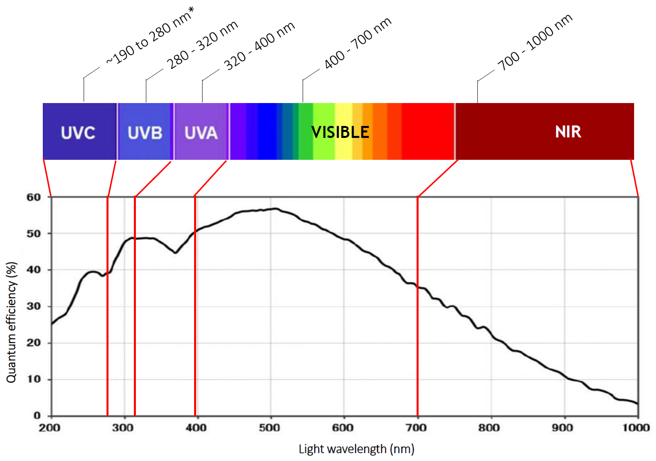
Spectral response of GO-8105M-5GE-UV
*Sensitivity extends below 200 nm but specific Quantum Efficiency has not yet been measured.
The broad UV spectral response shown above opens up the new camera to many UV-based machine vision applications. The biggest opportunities lie with companies building various types of semiconductor inspection systems, including the inspection of semiconductor masks. In semiconductor mask applications, for example, the capabilities of the new Go Series GO-8105M-5GE-UV camera can be used to inspect whether the photoresist agent is evenly applied on the semiconductor before exposure. These are expensive systems that are counted on to ensure the highest manufacturing quality. They need to use very short wavelengths to reveal the smallest surface features and detect defects on wafers, masks, and other related items. The OEMs who build these systems will find the UV capabilities of this new camera – extending well into the UVC band – to be quite attractive.
The GO-8105M-5GE-UV camera is also offered in a “glassless” configuration with a removable cover glass over the sensor to enable it to be used for laser profiling and any other applications where even UV-compatible quartz glass in the optical path might prove problematic.
In summary, UV cameras have become essential for a variety of industrial and scientific applications. However, while UV imaging has begun to emerge as an inspection tool for many industrial processes, the field is still in its infancy relative to visible or near-infrared-based machine vision. But the field of UV machine vision is growing as commercial UV hardware drops in price and increases in diversity.
Free white paper:
Explore the value of UV technology in detecting surface defects and inconsistencies in semiconductor microchip manufacturing.
Download free white paper
Contact JAI for help:
Let us help you to find the perfect camera to meet your application requirements for UV applications.
Contact a JAI engineer